Dear Umbra,
I read that thin-film solar panels are now being produced on a wider scale. I always hear that they can be sandwiched into window glass, but are there any companies that are actually using the technology in architectural products? How does thin film compare to the traditional PV panel?
Jen
Oakland, Calif.
Dearest Jen,
Thin films compare well to the traditional photovoltaic panel, and are commercially available in such form as roofing tiles, which I count as architectural products. That’s the short answer. The long, exhaustive answer you’ll have to read somewhere else — but I can give you the mid-sized, CliffsNotes answer. Umbra and Science, united once again in a zany matchup of wit and accuracy.

No s’mores over the campfire for these guys.
Photo: NASA
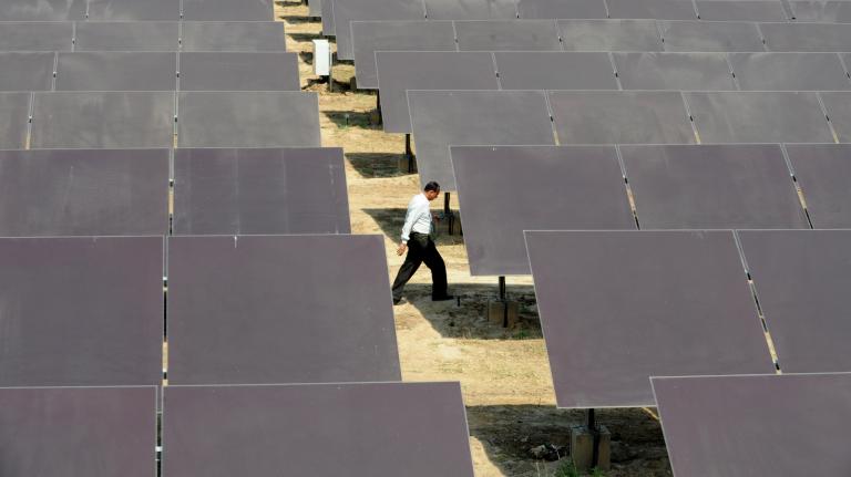
Thin films — which are known as such not because they appear thinner (though they do), but because their manufacturing process involves applying multiple thin layers of sun-transforming substance onto a base material — are themselves photovoltaic. They magically transform photons of light from the distant sun into voltage current that feeds our electrical systems. Not all solar energy is photovoltaic. Passive solar, in which you invite sun directly through windows and trap it in objects and the air, is not, and neither are solar water-heater systems. Traditional PV systems are the shiny black and silver squares of solar cells that you see linked together in giant rooftop slabs or atop roadside call boxes.
PV cells use the atomic properties of silicon (or other semiconductors) to trap energy, create electricity, and move that electricity through and out of the PV array into your home. I guess it’s not that important that we go over why silicon is a good element for this purpose, but I do have to mention the jargon: after “doping” the silicon with impurities such as boron, PV makers can create the perfect electricity-producing sun sandwich. Skipping how this happens — and editing out my professional-cycling doping imagery written to help you picture the process — is what allows this to be a short explanation. PV cells have been made from silicon for years because it is the perfect semiconductor. Turning silicon into PV cells is very energy intensive.
As I said, thin PV films are made by pasting layers onto a substrate (as opposed to the mysterious “ingot growth” and other methods of processing silicon). Other ways they compare to traditional silicon PV panels include: the conducting substance is not necessarily silicon, the manufacturing process may be less expensive, manufacturing can be automated and continuous — companies can and do make huge sheets and small sheets without too much trouble — and the use of flexible substrate means new potential uses. Such as, roofing tiles that look and act much like asphalt shingles, and glazing on skylights. Thin-film products are available for residential homes such as you yourself might own.
If you wish to read lots and lots more about how photovoltaic cells are made, or about doped silicon p-layer and n-layers, ingot growth, and physical vapor deposition, I really enjoyed the U.S. Department of Energy’s very thorough EERE site. A one-page description can be found at GE’s solar site, or at the National Renewable Energy Laboratory if you just want a wee bit more reading. I’ll gingerly touch the “but should I get some solar panels?” topic post haste.
Ingotly,
Umbra


